Full title of the thesis: Non Destructive Reverse Engineering of Printed Circuit Boards using
Micro Computed Tomography and Computer Vision
This post only aims to illustrate the main contents of the bachelor thesis, for the full overview, the original paper is best read in it’s full form.
Here is the abstract of the thesis:
Reverse engineering (RE) of printed circuit boards (PCBs) is used for a variety of purposes, such as in computer forensics and quality assurance. Usually RE is very labor-intensive or destructive, since it pertains either manually measuring all visible contacts, including desoldering the components for the covered pads and mapping them out individually, or the process is done by milling away layer by layer to see inside the object and uncover the traces. This thesis aims to automate the process as much as possible while being non-destructive. To achieve this, micro computed tomography (µ-CT) will be used to scan the PCB while information will be extracted with the help of computer vision.
The thesis researches the possibilities of using x-ray to reverse engineer PCBs. This makes it possible to understand PCBs without the need of damaging them using different methods.
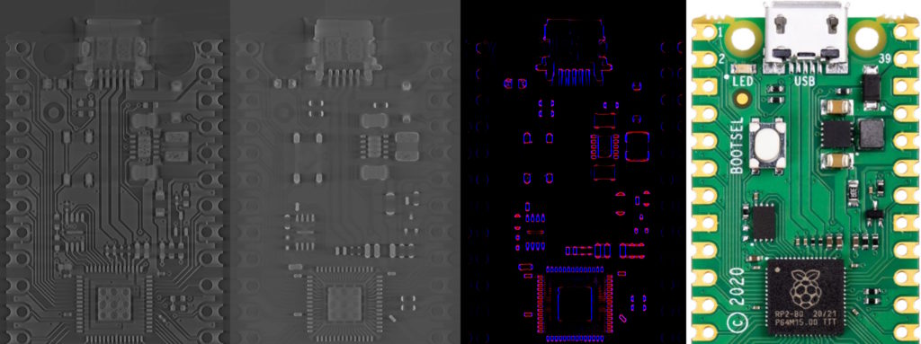
The program was not finished at the end of the thesis, since the reconstruction part was still missing, but the whole procedure was shown to work in theory. Here are a few pictures taken from the thesis to visualize the problems:
Left to right: CT scan, pre-processed CT scan, edge detection visualized, original picture
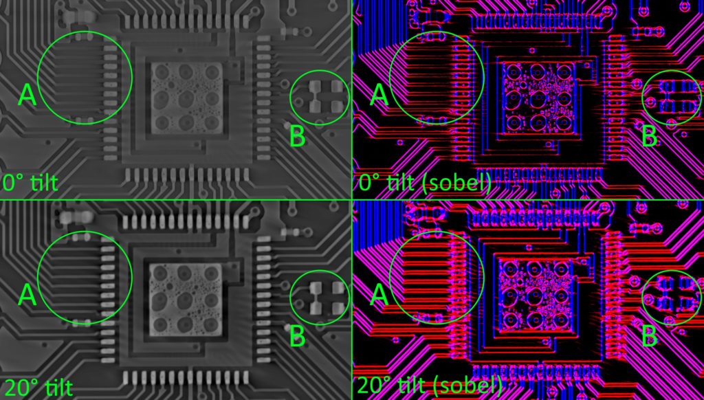
This is a comparison of the fix by tilting the PCBs when scanning in a certain way:
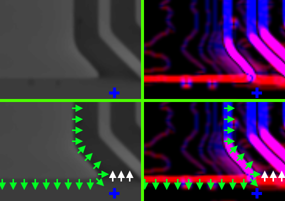
This picture shows the edge detection up close and explains the coloured lines:
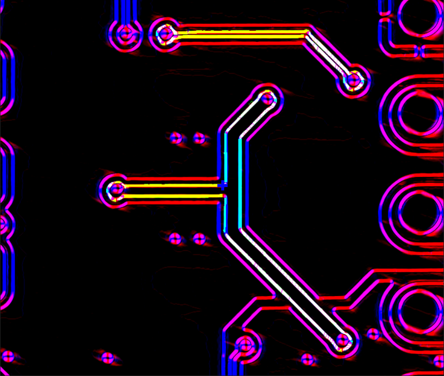
The picture below shows the algorithm recognizing two traces on the PCB